

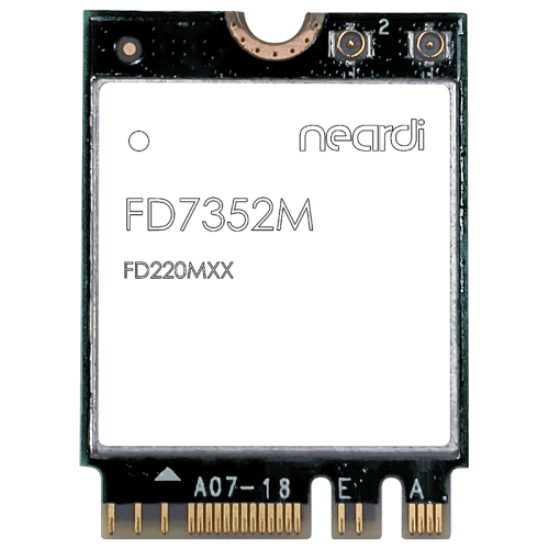
FD7352M
Interface: M.2 Key A-E
WiFi/Bluetooth: WiFi 6/6E; BT 5.4 Frequency Bands: 2.4G; 5G
Antenna: 2T2R
Maximum physical layer data rate for 2.4G/5G: 572.4Mbps/1.2Gbps
Bandwidth: 80MHz
Throughput: 1Gbps
Certifications: SRRC/ROHS/CE/FCC
Dimensions: 20mm*30mm

| TOP | |||
| Pin Number | Pin Name | Pin Type | Pin Description |
| 1 | GND | G | Ground connections |
| 3 | USB_DP | I/O | USB Transmitter/Receiver Differential Pair |
| 5 | USB_DM | I/O | USB Transmitter/Receiver Differential Pair |
| 7 | GND | G | Ground connections |
| 9 | NC | - | Floating |
| 11 | NC | - | Floating |
| 13 | NC | - | Floating |
| 15 | NC | - | Floating |
| 17 | NC | - | Floating |
| 19 | NC | - | Floating |
| 21 | NC | - | Floating |
| 23 | NC | - | Floating |
| 25 | NC | - | Floating |
| 27 | NC | - | Floating |
| 29 | NC | - | Floating |
| 31 | NC | - | Floating |
| 33 | GND | G | Ground connections |
| 35 | PERP0 | I | PCIe receive data-Positive |
| 37 | PERN0 | I | PCIe receive data-Negative |
| 39 | GND | G | Ground connections |
| 41 | PETP0 | O | PCIe receive data-Positive |
| 43 | PETN0 | O | PCIe transmit data-Negative |
| 45 | GND | G | Ground connections |
| 47 | REFCLKP0 | I | PCIe differential clock input-Positive |
| 49 | REFCLKN0 | I | PCIe differential clock input-Negative |
| 51 | GND | G | Ground connections |
| 53 | CLKREQ0#(3.3V) | O | PCIe clock request |
| 55 | PEWAKE0#(3.3V) | O | PCIE wake-up signal |
| 57 | GND | G | Ground connections |
| 59 | NC | - | Floating |
| 61 | NC | - | Floating |
| 63 | GND | G | Ground connections |
| 65 | NC | - | Floating |
| 67 | NC | - | Floating |
| 69 | GND | G | Ground connections |
| 71 | NC | - | Floating |
| 73 | NC | - | Floating |
| 75 | GND | G | Ground connections |
| BOTTOM | |||
| Pin Number | Pin Name | Pin Type | Pin Description |
| 2 | 3.3 V | P | Main power voltage source input |
| 4 | 3.3 V | P | Main power voltage source input |
| 6 | GPIO2(3.3V) | I/O | RESERVED |
| 8 | NC | - | Floating |
| 10 | NC | - | Floating |
| 12 | NC | - | Floating |
| 14 | NC | - | Floating |
| 16 | GPIO1(3.3V) | I/O | RESERVED |
| 18 | GND | G | 接地连接 |
| 20 | NC | - | Floating (Don’t connected to ground) |
| 22 | UART_TX(3.3V) | I/O | UART TX signal |
| 24 | NC | - | Floating |
| 26 | NC | - | Floating |
| 28 | NC | - | Floating |
| 30 | NC | - | Floating |
| 32 | UART_RX(3.3V) | I/O | UART RX signal |
| 34 | UART_RTS(3.3V) | I/O | UART DCE request to send signal |
| 36 | UART_CTS(3.3V) | I/O | UART DEC clear to send signal |
| 38 | CHIP_EN | I | Module enable signal(Internal 10K pull-up) |
| 40 | NC | - | Floating |
| 42 | NC | - | Floating |
| 44 | NC | - | Floating |
| 46 | NC | - | Floating |
| 48 | NC | - | Floating |
| 50 | NC | - | Floating |
| 52 | PERSTN#(3.3V) | I | PCIe host indication to reset the device |
| 54 | NC | - | Floating |
| 56 | NC | - | Floating |
| 58 | NC | - | Floating |
| 60 | NC | - | Floating |
| 62 | NC | - | Floating |
| 64 | NC | - | Floating |
| 66 | NC | - | Floating |
| 68 | NC | - | Floating |
| 70 | NC | - | Floating |
| 72 | 3.3 V | P | Main power voltage source input |
| 74 | 3.3 V | P | Main power voltage source input |

 Tel
Tel Email
Email Address